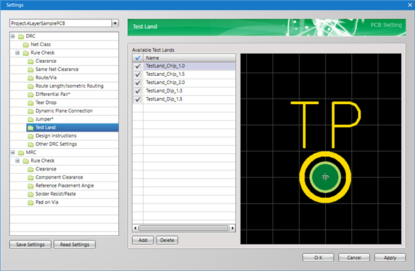
Kicad Test Point
Using eagle footprints in kicad if you're familiar with eagle, it can be scary to think all the time spent creating footprints will be lost when switching to. You may skip running it, but i recommend running the test.
Test point footprint does such a part exist? Layout KiCad.info Forums

Established in 1954, the organization is.

Kicad test point. Kicad est une suite logicielle de conception de cartes électroniques assistée par ordinateur. From proper grounding to material selection, common best practices for optimal rf results. Previously i could fudge a line in copper on a footprint, and as long as the line did not cross the centre point of a pad it was not spotted by the drc.
It is actually hosted in the source but could become a standalone project. An interesting phenomenon applied in the field of instrumentation is the seebeck effect, which is the production of a small voltage across the length of a wire due to a difference in temperature along that wire.this effect is most easily observed and applied with a junction of two dissimilar metals in contact, each metal producing a different seebeck voltage along its length. Can i create a pcb without creating schematic?
Kicad 6.0 is expected to arrive in the second quarter of 2021 and is the first major release since 2018. The goal of this document is to provide an overview for developers of the goals for the project for the version 6 release of kicad. Click to get the latest buzzing content.
Seth hillbrand 9 fix committed: Why do you need controlled impedance? Kicad caused me to start this again.
If this price is not low enough for you, here is a sbc based on d1s, the. Then, the links to the models within the layout (.kicad_pcb) file are modified so that they point to the archived 3d models with a path relative to the project folder. The new kicad does spot this, and so spots the antenna is a loop that shorts things.
Yes but for any but the simplest pcbs, please see: It’s a long, difficult journey to launch a new physical product. If this runs and your bit does not cut through the copper all the way around the board, you can adjust the zero point of the z axis and run the test again.
You can place a top/bottom layer pad , and then route it with track. Printed circuit design and fab online magazine. A global drc test is very strongly recommended.
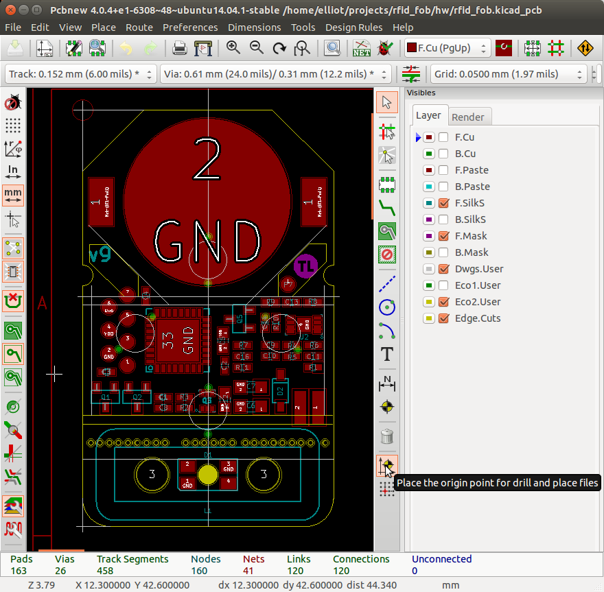
Although hardware is known for being hard, it’s. Kicad 6.0 roadmap this document is the kicad version 6 developer's road map document. In the 'place dxf origin (0,0) point:' option, select the placement of dxf origin relative to the board coordinates (the kicad board has (0,0) in the top left corner).
2 critical 9 fix committed: Ne jamais brancher une led à l'envers sous peine de la détruire car la tension inverse est relativement faible. I took much of january to play with the kicad nightly builds, tagged kicad 5.99, which will eventually become kicad 6.0.in this article, i document many of the most important changes that the kicad developers have introduced to kicad 6, including numerous.
Gerbv lets you load several files on top of each other, do measurements on the displayed image, etc. Organisation européenne pour la recherche nucléaire), known as cern (/ s ɜːr n /; Dsi is mostly used in mobile devices (smartphones & tablets).
A while back, [heavydeck] remembered stumbling across the worst cad package ever, which is a schematic editor whose existence was purely intended for use to make quick circuit sketches for document… When you open up kicad, you’ll see the window shown in image 2.1. If you have saved the schematic, you can still go back and run the rescue function again by selecting rescue cached components in the tools menu to call up the rescue dialog again.
The purpose of this gcode is to test the tool depth around the boundary of the work piece. When the plugin is run, eeschema has to be closed. Library maintainer rules & guidelines.
The european organization for nuclear research (french: In order to maintain the legibility of the kicad_pcb and pretty data files,. Prototyping is a big part of any electrical work because it is very meticulous and to the point.
I won’t lie to you, though. Circuit designers must test many times to make sure their design works efficiently and most of all is safe for a consumer to buy and use. 2 critical 9 fix committed:
The plugin is run from pcbnew. Radio waves are all the rage. Open source isa surely is an attractive title to geeks.
You can place a single pin connector from eelib, and then update its footprint. Setting grid origin in footprint library browser causes crash: Derived from the name conseil européen pour la recherche nucléaire), is a european research organization that operates the largest particle physics laboratory in the world.
If you save the schematic at this point, your cache will be overwritten and the old symbols will not be recoverable. Kicad crashes when cvpcb or footprint editor opens: It is living document that should be maintained during the version 6 development cycle.
Even if the kicad libraries contain the part, you'll want to check it against the datasheet very closely and do a one to one test print. Point important à retenir : Choose where you want to save your project and type in a name for it.
From here, you can open or create new projects. Kicadtools a proof of concept module to read kicad 6.kicad_sch schema file and compute the netlist. You won’t need any prior knowledge of electronics design to understand this article.
How to add test point in schematic or pcb? This module can be used to perform any kind of processings on a kicad schema. I started this project as the base for.
S'il n'y a aucune documentation il est raisonnable d'effectuer un test en branchant une led avec un branchement en série d'une réisistance d'environ 500 ohms et sous une tension de 3v maximum. Although, it will be easier to comprehend if you already have a technical background in computers, engineering or another field of science. Circuit design is a very rigorous job to do and get done without making a mistake.
I’ve been following the development of kicad for a number of years now, and using it as my main electronics cad package daily for a the last six years or thereabouts, so the release of kicad 6.0.
Kicad newbie how to add a test point (easily) Layout KiCad.info Forums

Kicad Test Point Footprint Circuit Boards
Kicad Test Point Footprint Circuit Boards

Kicad Test Point Footprint Circuit Boards

Kicad Test Point Footprint Circuit Boards

Kicad newbie how to add a test point (easily) Layout KiCad.info Forums

Kicad Test Point Footprint Circuit Boards

Kicad Test Point Footprint Circuit Boards
Kicad Test Point Footprint Circuit Boards

Test point footprint does such a part exist? Layout KiCad.info Forums

openfixturekicadexport Tiny Labs
Mismatch between hierachical labels and pin sheet Schematic KiCad.info Forums

Kicad Test Point Footprint Circuit Boards
Kicad Test Point Footprint Circuit Boards
openfixturekicadexport Tiny Labs
Kicad Test Point Footprint Circuit Boards

Kicad Test Point Footprint Circuit Boards
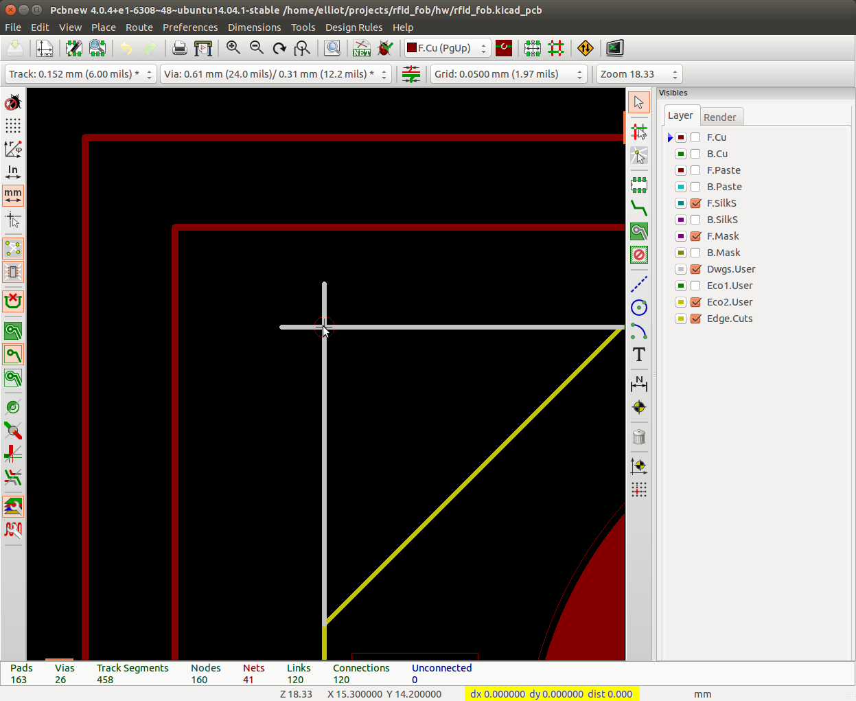
A weird test point on PCB? Layout KiCad.info Forums

Jumper pads for I2C addressing Footprints KiCad.info Forums
